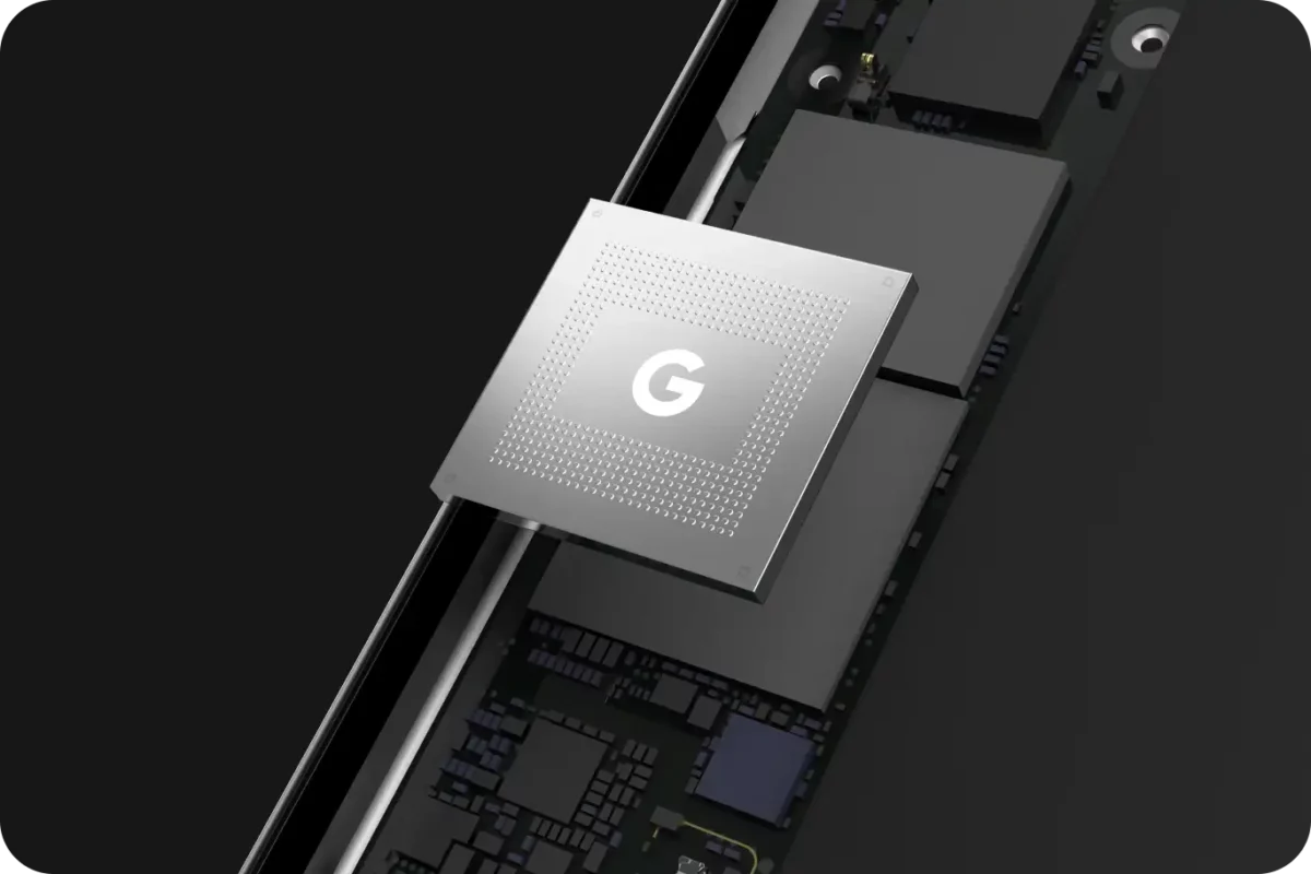
The Samsung-built Google Tensor G4 chip looks poised to bring Galaxy S24-like performance to Google’s Pixel 9 series in 2024…
TL;DR –Google’s Tensor G4 Chip: Big Gains Are Coming To Pixel 9 Series
- 🚀 Next-Gen Power: Pixel 9 series to feature Google’s Tensor G4 SoC, crafted by Samsung with a 4nm process.
- 🛠️ Samsung Manufacture: Same 4nm tech as Exynos 2400, aiming for reliability over Exynos’s spotty record.
- 🔧 Tech Advancements: Gains from Samsung’s FOWLP tech, boosting heat dissipation for higher performance.
- 🌡️ Cool & Fast: Enhanced thermal management allows for increased clock speeds and voltages.
- 📈 Performance Boost: Tensor G4 aims to match high-end phones like Galaxy S24 in speed and efficiency.
Google’s been working on its Tensor platform for a solid few years now. Performance has never been its strong suit, but the platform is getting better with each generation alongside its growing array of AI smarts.
And yet, despite this, Google’s Pixel 7 and Pixel 8 series have played second-fiddle to iPhone and Samsung phones with respect to overall performance. But in 2024, all of this is going to change – Google has closed the gap, according to reports.
Tensor G4 For Pixel 8 Series Bringing Galaxy S24-Like Performance

The Pixel 9 series will be powered by Google’s next-generation Tensor G4 system-on-chip (SoC). The G4 will be manufactured by Samsung Electronics’ foundry business using their 4nm process node, the same it uses for its current Exynos 2400 SoC.
Let’s just hope Google’s design is a little more reliable than Samsung’s always-in-the-news-for-all-the-wrong-reasons Exynos platform which has consistently been out-performed by its Snapdragon counterpart.
Where Are The Gains Coming From?
The big improvements come via Samsung’s adoption of fan-out wafer-level packaging (FOWLP) for the chips’ fabrication process.
This packaging technology provides better heat dissipation which means the chipset can run at higher clock speeds and voltages while maintaining thermal limits.
Or, if you’d prefer, here’s a more “technical” overview of how (FOWLP) works in practice:
- Die Placement: The process begins with the placement of one or more semiconductor dies (the bare chips that contain the integrated circuits) on an adhesive film. These dies are placed face-down, and there is no need for a carrier substrate, which is typically used in other packaging methods.
- Molding: Once the dies are in place, they are encapsulated with a mold compound. This encapsulation provides mechanical support and protects the dies from external damage or contamination.
- Fan-Out Process: After encapsulation, the key feature of FOWLP comes into play—the fan-out process. This involves creating a re-distributed layer (RDL) around the dies. The RDL is essentially a network of new wiring routes that fan out from the original die pads. This step allows for more connections and can integrate additional passive components directly into the package.
- Ball Grid Array (BGA): The bottom side of the package is then prepared with a ball grid array (BGA). This array consists of solder balls that are used to connect the packaged chip to a circuit board. The arrangement and density of these solder balls can be customized based on the specific requirements of the device it will be mounted on.
- Finalization: The package is completed with the application of a protective coating and any required testing to ensure functionality and reliability.
By leveraging the more advanced 4nm process and FOWLP packaging from Samsung, the Tensor G4-powered Pixel 9 and Pixel 9 Pro should – theoretically – be closer to the Samsung Galaxy S24 series and other high-end Android phones with respect to overall performance and speed.
Add in the raft of improvements Google is rumored to be making to the Pixel 9’s camera tech, its ever-evolving AI smarts, and the fact that Google’s Pixel 9 series will be cheaper than Apple and Samsung’s top-shelf gear, and things are looking pretty good for Pixel fans in 2024.
Next Up: Samsung’s 3nm Process For Pixel 10 In 2025
Looking ahead, Samsung’s next generation 3nm gate-all-around transistor processes may be employed for both Exynos and Tensor chipsets in the future, potentially allowing further performance and efficiency gains.
The Pixel 10 in 2025 could be one of the first smartphones to benefit from this cutting-edge 3nm process technology for mobile silicon.
The Google Pixel 9 series is expected to launch in October 2024. Google’s more affordable Pixel 8a is rumored for a mid-2024 release, while a follow-up to the Pixel Fold could potentially debut sometime in 2024 as well.


